| CPC H01L 23/535 (2013.01) [H01L 21/76805 (2013.01); H01L 21/76816 (2013.01); H01L 21/76829 (2013.01); H01L 21/76895 (2013.01); H01L 23/5283 (2013.01); H10B 43/50 (2023.02); H10B 41/50 (2023.02); H10B 43/27 (2023.02)] | 22 Claims |

|
1. An integrated circuit comprising:
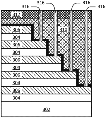
a memory staircase structure, wherein first and second steps included in the staircase structure each comprises an insulator material layer and a conductive material layer;
an etch stop on the staircase structure, the etch stop including a high-k dielectric material, wherein the etch stop is a multi-layer structure that includes a first layer and a second layer, and one or both of the first and second layers comprises multiple phases;
an insulator fill material on the etch stop;
a first contact that passes through the etch stop and is on the conductive material layer of the first step, wherein the first contact has a first height; and
a second contact that passes through the etch stop and is on the conductive material layer of the second step, wherein the second contact has a second height that is more than 5× greater than the first height.
|