| CPC H01L 23/528 (2013.01) [H01L 23/481 (2013.01); H01L 23/5386 (2013.01); H01L 23/585 (2013.01); H01L 25/0652 (2013.01); H01L 25/0655 (2013.01); H01L 21/78 (2013.01); H01L 22/20 (2013.01); H01L 24/05 (2013.01); H01L 24/06 (2013.01); H01L 24/08 (2013.01); H01L 24/30 (2013.01); H01L 24/32 (2013.01); H01L 2224/0557 (2013.01); H01L 2224/06181 (2013.01); H01L 2224/08145 (2013.01); H01L 2224/08225 (2013.01); H01L 2224/30181 (2013.01); H01L 2224/32145 (2013.01); H01L 2224/32225 (2013.01)] | 16 Claims |

|
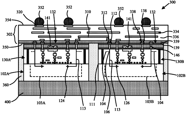
1. A multi-die structure including:
a routing layer including a first package-level bond pad, a second package-level bond pad, and a package-level die-to-die routing electrically connecting the first package-level bond pad to the second package-level bond pad;
a first die bonded to a first side of the routing layer and in electrical connection with the first package-level bond pad; and
a second die bonded to the first side of the routing layer and in electrical connection with the second package-level bond pad;
wherein the first die includes:
a first front-end-of-the-line (FEOL) die area including a communication device selected from the group consisting of a transceiver and a receiver; and
a first back-end-of-the-line (BEOL) build-up structure spanning over the first FEOL die area, the first BEOL build-up structure including an intra-chip routing connected to the communication device, and a chip-level die-to-die routing connecting the communication device to a first bond pad of the first BEOL build-up structure, wherein the first bond pad is bonded to the routing layer and electrically connected to the first package-level bond pad.
|