| CPC H01L 23/528 (2013.01) [H01L 23/5226 (2013.01); H10B 41/27 (2023.02); H10B 43/27 (2023.02)] | 11 Claims |

|
1. A semiconductor storage device, comprising:
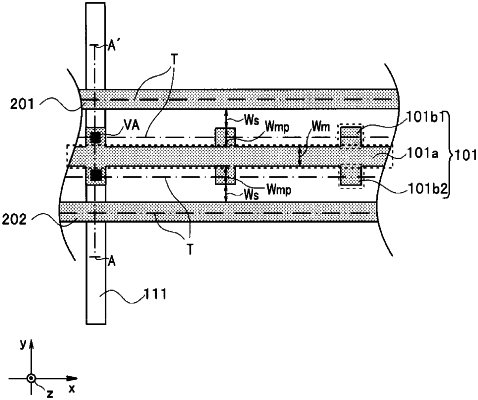
a first signal line extending in a first direction;
a second signal line extending in the first direction and adjacent to the first signal line in a second direction orthogonal to the first direction; and
a third signal line extending in the second direction in a second wiring layer different from a first wiring layer in which the first signal line is disposed, wherein
the first signal line includes:
a trunk wiring extending in the first direction that includes two branch wirings at a particular position of the trunk wiring, the two branch wirings including a first branch wiring extending from one side of the trunk wiring toward the second signal line in the second direction and a second branch wiring extending from another side of the trunk wiring in the second direction, wherein each of the first branch wiring and the second branch wiring includes a connection portion that electrically connects the first signal line and the third signal line.
|