| CPC H01L 23/49838 (2013.01) [H01L 21/486 (2013.01); H01L 23/147 (2013.01); H01L 23/49827 (2013.01); H01L 23/49866 (2013.01)] | 9 Claims |

|
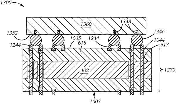
1. A semiconductor device assembly, comprising:
a silicon core structure comprising:
a first side opposing a second side;
at least one via, the at least one via comprising a via surface extending between the first side and the second side; and
a metal cladding layer formed on and in direct contact with the first side, the second side, and the via surface, the metal cladding layer extending along the via surface between the first side and the second side;
a dielectric layer formed over the metal cladding layer on the first side, the second side, and the via surface, the dielectric layer extending along the metal cladding layer between the first side and the second side;
a conductive interconnection formed through the at least one via of the silicon core structure and having a surface exposed at the first side and the second side;
a first redistribution layer formed over the first side; and
a second redistribution layer formed over the second side, wherein the first redistribution layer and the second redistribution layer each have one or more conductive contacts formed thereon, and wherein the metal cladding layer is conductively coupled to ground or a reference voltage by at least one of the one or more conductive contacts formed on the first redistribution layer and the second redistribution layer, wherein the metal cladding layer has a thickness between about 100 nm and about 5 μm on substantially all exposed surfaces of the silicon core.
|