| CPC H01L 23/49562 (2013.01) [H01L 21/4825 (2013.01); H01L 21/4828 (2013.01); H01L 23/3142 (2013.01); H01L 23/4824 (2013.01); H01L 23/4951 (2013.01); H01L 23/49568 (2013.01); H01L 23/544 (2013.01); H01L 23/562 (2013.01); H01L 2223/54426 (2013.01); H01L 2223/54486 (2013.01); H01L 2224/26175 (2013.01); H01L 2224/27013 (2013.01); H01L 2224/32258 (2013.01)] | 13 Claims |

|
1. A semiconductor device package, comprising:
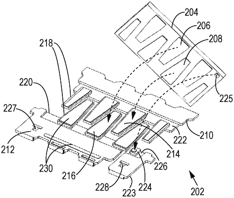
a leadframe, the leadframe having a first portion with first extended portions and a second portion with second extended portions, the first portion being entirely physically disconnected from the second portion, the first extended portions being interdigitated with the second extended portions along an axis, wherein the first portion includes a first recessed portion with the first extended portions connected thereto, the first recessed portion having a top surface that is recessed below a first surface of the first extended portions, the first recessed portion extending at least partially around three sides of each of the first extended portions, and the second portion includes a second recessed portion with the second extended portions connected thereto, the second recessed portion having a top surface that is recessed below a first surface of the second extended portions, the second recessed portion extending at least partially around three sides of each of the second extended portions, wherein each of the first extended portions is spaced from the second recessed portion in a direction perpendicular to the axis, and each of the second extended portions is spaced from the first recessed portion in the direction perpendicular to the axis;
mold material encapsulating at least a portion of the leadframe and at least a portion of a semiconductor die electrically mounted to the leadframe, the semiconductor die having a first set of contacts alternated with a second set of contacts, with the first set of contacts connected to the first surface of the first extended portions and the second set of contacts connected to the first surface of the second extended portions; and
a mold-locking cavity having the mold material included therein and in contact with a second surface of the first extended portions opposed to the first surface of the first extended portions, a second surface of the second extended portions opposed to the first surface of the second extended portions, the first portion of the leadframe, and the second portion of the leadframe.
|