| CPC H01L 21/823412 (2013.01) [H01L 21/02112 (2013.01); H01L 21/02225 (2013.01); H01L 21/02282 (2013.01); H01L 21/02321 (2013.01); H01L 21/02343 (2013.01); H01L 21/823437 (2013.01); H10B 41/27 (2023.02); H10B 43/27 (2023.02)] | 18 Claims |

|
1. Integrated circuitry comprising:
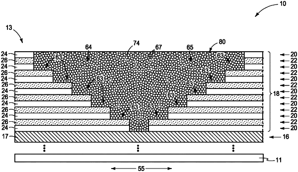
a three-dimensional (3D) array comprising tiers of electronic components;
a stair-step structure laterally-adjacent the 3D array, the stair-step structure having steps individually comprising a tread and a riser; and
insulating material atop individual of the treads and aside individual of the risers, the insulating material comprising:
touching insulative physical objects having void-spaces there-among, the insulative physical objects individually having at least one of a maximum submicron dimension or a minimum submicron dimension, a plurality of the insulative physical objects being both vertically and laterally offset relative to one another, the insulative physical objects comprising at least one of (a) or (b), where:
(a): nanowires having two straight-line dimensions therethrough from 1 to 100 nanometers and an aspect ratio of 100 to 1,000; and
(b): nanorods having two straight-line dimensions therethrough from 1 to 100 nanometers and an aspect ratio of 2 to 99; and
solid insulative material in the void-spaces.
|