| CPC H01L 21/76898 (2013.01) [H01L 23/481 (2013.01); H01L 25/0657 (2013.01); H01L 25/50 (2013.01); H01L 23/5329 (2013.01); H01L 2225/06544 (2013.01)] | 22 Claims |

|
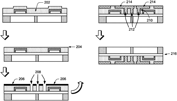
1. A method for fabricating a plurality of through-dielectric vias (TDVs) in a chip-to-wafer process, wherein the plurality of TDVs is formed through a dielectric block of an integrated circuits assembly, and the dielectric block is formed between adjacent devices of a substrate comprising a silicon wafer and a plurality of devices formed on the silicon wafer, the plurality of devices comprising the adjacent devices, the method comprising:
(a) removing a section of the silicon wafer disposed between the adjacent devices, wherein:
the section is removed from a first side of the substrate to a depth that extends to an opposite second side of the substrate;
a plurality of chips is attached to the second side; and
one or more of the plurality of chips are communicatively coupled to one or more devices of the plurality of devices through a back-end-of-line (BEOL) distribution layer disposed between the second side and the plurality of chips;
(b) after (a), depositing a dielectric material on the first side of the substrate and planarizing the dielectric material to form a dielectric layer, wherein:
a first portion of the dielectric layer comprises the dielectric block and second portions of the dielectric layer are disposed over each of the plurality of devices; and
the dielectric block fills a space formed by removing the section at (a);
(c) forming a plurality of via holes through the dielectric block, wherein the plurality of via holes extend from the first side to the second side of the substrate; and
(d) metalizing the plurality of via holes to form the plurality of TDVs.
|