| CPC H01L 21/76895 (2013.01) [H01L 21/76805 (2013.01); H01L 21/76843 (2013.01); H01L 21/76879 (2013.01); H01L 23/53233 (2013.01); H01L 23/53238 (2013.01); H01L 23/535 (2013.01)] | 12 Claims |

|
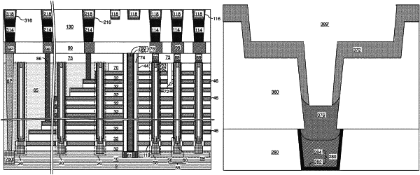
1. A semiconductor structure, comprising:
a first dielectric material layer;
a first metal interconnect structure embedded within the first dielectric material layer and comprising a first metallic material portion including a first metal;
a second dielectric material layer located over the first dielectric material layer;
a second metal interconnect structure embedded within the second dielectric material layer and comprising an integrated line-and-via structure that includes a second metallic material portion comprising a second metal, wherein the integrated line-and-via structure comprises a metallic line portion and a metallic via portion adjoined to and underlying the metallic line portion; and
a metal-semiconductor alloy portion comprising a first metal-semiconductor alloy of the first metal and a semiconductor material is located underneath the second metallic material portion, and contacts a top surface of the first metal interconnect structure;
wherein:
a bottommost surface segment of the metal-semiconductor alloy portion is located below a horizontal plane including an interface between the first dielectric material layer and the second dielectric material layer; and
a top surface of the metal-semiconductor alloy portion is located above the horizontal plane including the interface between the first dielectric material layer and the second dielectric material layer.
|