| CPC H01L 21/76831 (2013.01) [H01L 21/76822 (2013.01); H01L 23/49894 (2013.01); H01L 23/5329 (2013.01); H01L 23/15 (2013.01); H01L 23/49822 (2013.01); H01L 23/49827 (2013.01); H01L 23/5226 (2013.01); H01L 23/5384 (2013.01)] | 18 Claims |

|
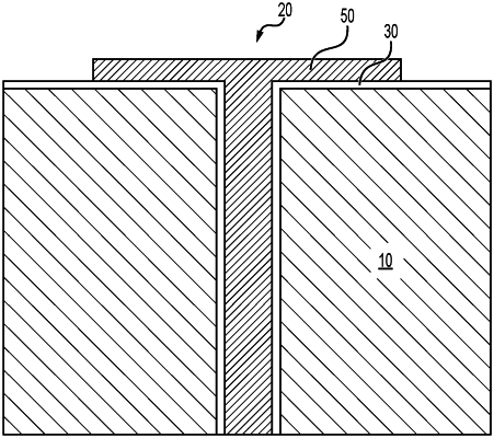
1. A method of improving interfacial adhesion of a copper-glass interface in a Through Glass Via (TGV) of an electronic device, comprising:
providing a glass substrate with a plurality of TGVs formed thereon;
forming a coating of a curable polymer material on an internal wall of a TGV of the plurality of TGVs, wherein a viscosity of the curable polymer material is less than 30 Poise;
curing the coating of the curable polymer material to form a dielectric liner having a tensile strength greater than about 8 Mpa and a dielectric loss less than about 0.002; and
depositing a layer of copper on the dielectric liner.
|