| CPC H01L 21/76289 (2013.01) [H01L 21/76813 (2013.01)] | 20 Claims |

|
1. A method of forming a semiconductor device, comprising:
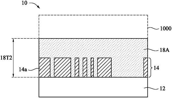
forming a plurality of non-insulator structures on a substrate, the plurality of non-insulator structures being spaced apart by trenches;
forming a sacrificial layer overfilling the trenches;
reflowing the sacrificial layer at an elevated temperature, wherein a top surface of the sacrificial layer after the reflowing is lower than a top surface of the sacrificial layer before the reflowing, and a middle of a first segment of the top surface of the sacrificial layer between two of the plurality of non-insulator structures after the reflowing is at a same elevation as a second segment of the top surface of the sacrificial layer directly over one of the plurality of non-insulator structures after the reflowing;
etching back the sacrificial layer to lower the top surface of the sacrificial layer to fall below top surfaces of the plurality of non-insulator structures;
forming a dielectric layer on the sacrificial layer; and
removing the sacrificial layer to form air gaps below the dielectric layer.
|