| CPC H01L 21/6875 (2013.01) [C23C 4/02 (2013.01); C23C 4/134 (2016.01); H01L 21/68757 (2013.01)] | 3 Claims |

|
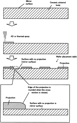
1. A wafer placement table which is a ceramic sintered body with a surface provided with multiple projections that support a wafer,
wherein of the surface of the ceramic sintered body, an area provided with no projection is a mirror surface which has a surface roughness Ra of 0.1 μm or less, and
the projections are formed of an aerosol deposition film or a thermal spray film made of the same material as for the ceramic sintered body, and
wherein the projections have a denseness lower than a denseness of the ceramic sintered body.
|