| CPC H01L 21/32136 (2013.01) [H10B 41/27 (2023.02); H10B 41/35 (2023.02); H10B 43/27 (2023.02); H10B 43/35 (2023.02)] | 20 Claims |

|
1. A method of etching comprising:
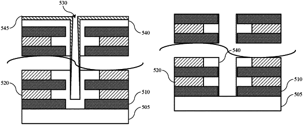
depositing a metal-containing material or a carbon-containing material along surfaces of an exposed metal within a high aspect-ratio structure defined on a substrate;
flowing a fluorine-containing precursor and a secondary gas into a processing region of a semiconductor processing chamber, wherein the secondary gas comprises oxygen or nitrogen, and wherein a flow rate ratio of the fluorine-containing precursor to the secondary gas is greater than or about 1:1;
contacting the substrate with the fluorine-containing precursor and the secondary gas; and
etching the exposed metal within the high aspect-ratio structure.
|
|
12. A method of etching comprising:
depositing a metal-containing material or a carbon-containing material along surfaces of an exposed metal within a high aspect-ratio structure defined on a substrate;
flowing a first fluorine-containing precursor and a secondary gas into a processing region of a semiconductor processing chamber;
contacting the substrate with the first fluorine-containing precursor and the secondary gas, wherein the substrate comprises an exposed metal, and wherein the substrate defines a memory hole in a 3D NAND structure, and wherein the exposed metal extends laterally into recesses formed perpendicular to the memory hole;
etching the exposed metal within the memory hole;
forming a plasma of an oxygen-containing precursor;
contacting the exposed metal with plasma effluents of the oxygen-containing precursor to produce oxidized metal;
flowing a second fluorine-containing precursor into the processing region of the semiconductor processing chamber; and
removing the oxidized metal.
|
|
20. A method of etching comprising:
depositing a metal-containing material or a carbon-containing material along surfaces of an exposed metal within a high aspect-ratio structure defined on a substrate;
flowing a first fluorine-containing precursor and a secondary gas into a processing region of a semiconductor processing chamber, wherein the secondary gas comprises oxygen or nitrogen;
contacting the substrate with the first fluorine-containing precursor and the secondary gas, wherein the substrate comprises an exposed metal, and wherein the substrate defines a high aspect-ratio structure;
etching the exposed metal within the high aspect-ratio structure;
contacting the exposed metal with an oxygen-containing precursor to produce oxidized metal;
flowing a second fluorine-containing precursor into the processing region of the semiconductor processing chamber; and
removing the oxidized metal, wherein the method is performed with a chamber operating temperature of less than or about 500° C.
|