| CPC H01L 21/0217 (2013.01) [H01L 21/02164 (2013.01); H01L 21/02211 (2013.01); H01L 21/02274 (2013.01); H01L 21/0234 (2013.01); H01L 21/31111 (2013.01); H01L 27/088 (2013.01); H10B 43/20 (2023.02); H10B 43/35 (2023.02)] | 20 Claims |

|
1. A method comprising:
providing a substrate having alternating oxide layers and nitride layers arranged in a staircase pattern comprising exposed horizontal nitride surfaces and exposed oxide and nitride sidewall surfaces;
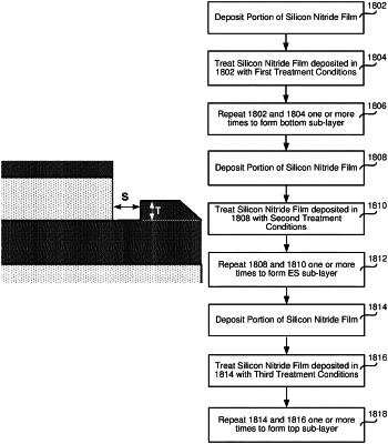
depositing a silicon nitride (SiN) layer over the alternating oxide and nitride layers by a plasma enhanced chemical vapor deposition (PECVD) process using a plasma generated from a process gas comprising a silicon-containing precursor; and
treating the SiN layer to selectively densify the SiN layer deposited on the exposed horizontal nitride surfaces wherein the SiN layer comprises a first sub-layer disposed between two second sub-layers each having a higher wet etch rate (WER) than the first sub-layer.
|