| CPC H01J 37/32183 (2013.01) [H01J 37/32091 (2013.01); H01J 37/32642 (2013.01); H01L 21/3065 (2013.01)] | 14 Claims |

|
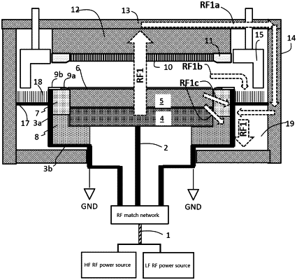
1. A plasma reactor, comprising:
a process chamber having a top, a bottom and a sidewall, a base is provided at the bottom, the base being connected to a radio-frequency RF power source via a RF match network, wherein a to-be-processed wafer is held above the base, an upper electrode assembly is provided at the top of the process chamber, and a plasma processing space is located between the base and the upper electrode assembly;
a first conductive ground ring surrounding the outer periphery of the base;
a second conductive ground ring connected between an outer sidewall of the first conductive ground ring and the sidewall of the process chamber, a plurality of gas channels being provided on the second conductive ground ring such that gas in the plasma processing space is exhausted through the plurality of gas channels;
an insulating ring provided between the base and the first conductive ground ring, wherein dielectric constant of the insulating ring is less than 3.5.
|