| CPC G11C 7/24 (2013.01) [G06F 3/0604 (2013.01); G06F 3/0655 (2013.01); G06F 3/0673 (2013.01); G11C 13/0023 (2013.01); G11C 13/0069 (2013.01); G11C 13/0097 (2013.01)] | 20 Claims |

|
1. An electronic device, comprising:
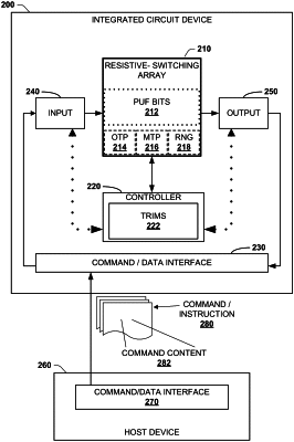
a resistive switching memory array comprising a plurality of resistive switching memory cells;
an interface configured to receive at the electronic device a communication from a host device that is external to the electronic device, wherein the communication includes first data indicative of an address of a group of memory cells of the plurality of resistive switching memory cells of the resistive switching memory array for implementing a memory command and second data specifying the memory command from a set of memory commands;
a set of trims that store instructions for configuring the resistive switching memory array to implement memory commands of the set of memory commands and for executing the memory command, wherein the set of trims includes a first trim defining a configuration of the resistive switching memory array and of program signal characteristics for implementing a physical unclonable feature (PUF) write command for the group of memory cells; and
a memory controller configured to:
determine whether the memory command is the PUF write command; and
implement the PUF write command on a set of native resistive switching memory cells of the plurality of resistive switching memory cells that includes at least the group of memory cells in response to the memory command being the PUF write command.
|