| CPC G11C 7/222 (2013.01) [G11C 7/1069 (2013.01); G11C 7/20 (2013.01)] | 20 Claims |

|
1. A memory system comprising:
a semiconductor storage device; and
a memory controller, wherein
the semiconductor storage device includes:
a power supply pad to which power is supplied;
a first signal pad to which a first signal is input;
a second signal pad to which a second signal is input;
a third signal pad to which a third signal is input;
a fourth signal pad to which a fourth signal is input;
a memory cell array;
a data register in which data read from the memory cell array are stored; and
a control circuit capable of executing a data-out operation of outputting data stored in the data register through the fourth signal pad, and
the memory controller is configured to:
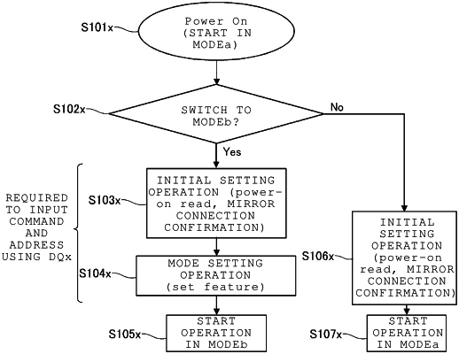
perform a mode setting operation by toggling the third signal input to the third signal pad, after at least one of the first signal input to the first signal pad and the second signal input to the second signal pad has been switched from a first level to a second level at a first timing after supplying power to the power supply pad,
perform an initial setting operation by transmitting a power-on read command to the semiconductor storage device at a second timing after the first timing, and
transmit a data-out command to the semiconductor storage device, at a third timing after the second timing, wherein
the semiconductor storage device receives the power-on read command and the data-out command via the first signal pad and the second signal pad.
|