| CPC G11C 7/1084 (2013.01) [G11C 7/109 (2013.01); G11C 7/1093 (2013.01); G11C 7/1096 (2013.01)] | 24 Claims |

|
18. A memory device, comprising:
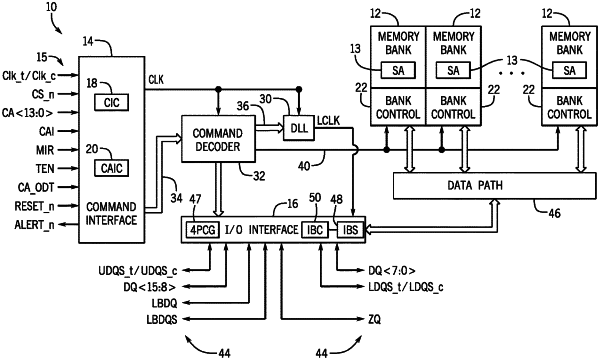
a command interface configured to receive write commands in an even pipeline and an odd pipeline from a host device;
a data strobe (DQS) input buffer configured to buffer a DQS signal from the host device;
a first ripple counter configured to suppress resets of the DQS input buffer while the first ripple counter is counting before reaching a threshold;
a second ripple counter configured to suppress resets of the DQS input buffer while the second ripple counter is counting before reaching the threshold; and
command handling circuitry, comprising:
clock domain shifting circuitry configured to shift commands received in the odd pipeline to a clock domain of the even pipeline;
stop count circuitry configured to stop counting in the first ripple counter or the second ripple counter if a subsequent write command is received before the respective ripple counter has reached the threshold; and
start count circuitry configured to start counting in the first ripple counter or the second ripple counter when a write command is received in the command interface.
|