| CPC G11C 7/1045 (2013.01) [G11C 5/025 (2013.01); G11C 7/1039 (2013.01); G11C 11/4087 (2013.01); G11C 11/409 (2013.01)] | 20 Claims |

|
1. A memory device comprising:
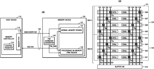
a memory cell array including a first memory region and a second memory region;
a processing-in-memory (PIM) engine configured to perform an internal processing operation on the first memory region;
a mode selector circuit configured to activate a processing mode selection signal for controlling the memory device to enter an internal processing mode when first addresses are received sequentially along with sequential write commands and when bit values of the first addresses match bit values of a first back-to-back address sequence of a PIM mode entering code associated with the sequential write commands, the PIM mode entering code being stored in the mode selector circuit; and
a command converter circuit configured to convert a received command into a PIM command to perform the internal processing operation in response to the activation of the processing mode selection signal.
|