| CPC G11C 29/4401 (2013.01) [G11C 29/1201 (2013.01); G11C 29/20 (2013.01); G11C 29/32 (2013.01); G11C 2029/1204 (2013.01)] | 22 Claims |

|
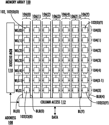
1. A memory array, comprising:
a first memory column circuit comprising:
a plurality of memory bit cells each contained in a respective memory row circuit of a plurality of memory row circuits; and
a counter circuit; and
for each scan cycle of a plurality of scan cycles of a scan mode:
the memory array is configured to
receive a next write input data from a serialized test data stream;
the counter circuit is configured to:
generate a next write value; and
generate a next read value offset from the next write value by a fixed offset value;
the memory array further configured to:
index a first memory row circuit of the plurality of memory row circuits at a memory address corresponding to the next write value;
write the next write input data to a first memory bit cell of the plurality of memory bit cells in the indexed first memory row circuit;
index a second memory row circuit of the plurality of memory row circuits at a memory address corresponding to the next read value; and
read a next read output data stored in second memory bit cell of the plurality of memory bit cells in the indexed second memory row circuit, on a read data output.
|