| CPC G11C 16/3427 (2013.01) [G11C 16/0483 (2013.01); G11C 16/08 (2013.01); G11C 16/14 (2013.01); G11C 16/24 (2013.01); G11C 16/3445 (2013.01); H01L 25/0657 (2013.01); H01L 2225/06562 (2013.01)] | 20 Claims |

|
1. An apparatus comprising:
one or more control circuits configured to connect to a three-dimensional memory structure having NAND strings, wherein each NAND string comprises memory cells, a drain side select gate, and a source side select gate, wherein the drain side select gate comprises a plurality of select transistors, wherein the three-dimensional memory structure further comprises word lines connected to control gates of the memory cells, bit lines associated with the NAND strings, and source lines associated with the NAND strings, wherein the one or more control circuits are configured to:
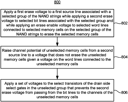
apply a first erase voltage to a first source line associated with a selected group of the NAND strings while applying a second erase voltage to selected bit lines associated with the selected group and while applying an erase enable voltage to selected word lines connected to selected memory cells on the selected group of the NAND strings to erase the selected memory cells; and
prevent erase of unselected memory cells while erasing the selected memory cells, wherein the unselected memory cells reside on an unselected group of NAND strings that shares the selected bit lines, including:
raise a potential of channels of the unselected memory cells to a first voltage of a second source line associated with the unselected group of NAND strings, wherein the first voltage has a sufficiently low magnitude to not erase the unselected memory cells given a second voltage on the word lines connected to the unselected memory cells; and
apply a set of voltages to the plurality of select transistors of the drain side select gates in the unselected group that prevents the second erase voltage from passing from the selected bit lines to the channels of the unselected memory cells, wherein voltages in the set of voltages decrease in a direction from the selected bit lines to the unselected memory cells.
|