| CPC G11C 16/26 (2013.01) [G11C 16/0483 (2013.01); G11C 16/08 (2013.01); G11C 16/10 (2013.01); G11C 16/3459 (2013.01); H01L 24/05 (2013.01); H01L 24/08 (2013.01); H01L 25/0657 (2013.01); H01L 25/18 (2013.01); H10B 41/27 (2023.02); H10B 43/27 (2023.02); H01L 2224/05147 (2013.01); H01L 2224/08145 (2013.01); H01L 2924/1431 (2013.01); H01L 2924/14511 (2013.01)] | 27 Claims |

|
1. A non-volatile memory device comprising:
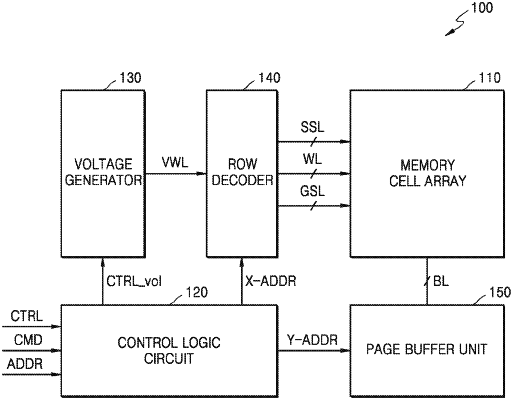
a memory cell array comprising a plurality of word lines; and
a control logic circuit configured to apply a first target voltage level to a selected word line as a selected word line voltage for a first sensing operation in a first sensing time and apply a second target voltage level to the selected word line as the selected word line voltage for a second sensing operation in a second sensing time,
the control logic circuit further configured to
set the selected word line voltage to be a first voltage level in a first section of the first sensing time,
set the selected word line voltage to be a second voltage level in a second section of the first sensing time which follows the first section of the first sensing time, wherein the second voltage level is less than the first voltage level,
set the selected word line voltage to be the first target voltage level in a third section of the first sensing time which follows the second section of the first sensing time, wherein the first target voltage level is greater than the second voltage level,
set the selected word line voltage to be a third voltage level in a first section of a second sensing time which follows the third section of the first sensing time, and
set the selected word line voltage to be the second target voltage level in a second section of the second sensing time which follows the first section of the second sensing time,
wherein the first target voltage level is greater than the second target voltage level, and
wherein the second target voltage level is greater than the third voltage level.
|