| CPC G11C 16/08 (2013.01) [G11C 16/0483 (2013.01); G11C 16/10 (2013.01); G11C 16/32 (2013.01); H10B 41/10 (2023.02); H10B 41/27 (2023.02); H10B 43/10 (2023.02); H10B 43/27 (2023.02)] | 6 Claims |

|
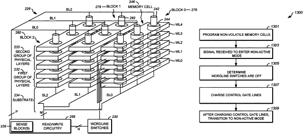
1. A method of delaying charge leakage in a word line of a nonvolatile memory, comprising:
storing data in a plurality of nonvolatile memory cells configured to store multiple data states;
using a word line to access selected ones of the non-volatile memory cells;
supplying a control gate signal on a control gate line;
controlling the conductivity of a word line switch connected between the word line and the control gate line to control the potential applied to the word line from the control gate line;
when entering a non-ON mode, placing all of word line switches in a nonconducting state and charging the control gate line to a charged potential.
|