| CPC G11C 11/418 (2013.01) | 33 Claims |

|
1. A circuit, comprising:
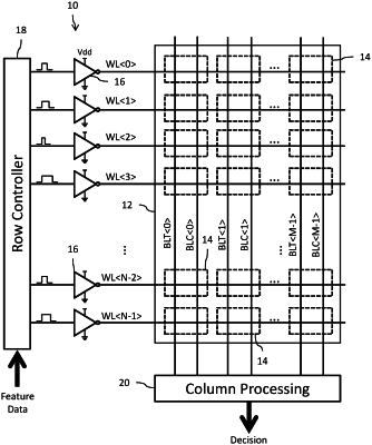
a memory array storing weight data for an in-memory compute operation and including a plurality of static random access memory (SRAM) cells arranged in a matrix with plural rows and plural columns, each column including a pair of bit lines connected to the SRAM cells of the column, and each row including:
a first word line configured to drive a first passgate transistor of the SRAM cell coupled between a first data storage node of the SRAM cell and one bit line of the pair of bit lines; and
a second word line configured to drive a second passgate transistor of the SRAM cell coupled between a second data storage node of the SRAM cell and another bit line of the pair of bit lines;
a first word line driver circuit for each row having an output connected to drive the first word line of the row;
a second word line driver circuit for each row having an output connected to drive the second word line of the row;
a row controller circuit configured to simultaneously actuate only the first word lines in a first phase of the in-memory compute operation by applying pulses having pulse widths modulated by feature data of the in-memory compute operation through the first word line driver circuits to the first word lines and then simultaneously actuate only the second word lines in a second phase of the in-memory compute operation by applying pulses having pulse widths modulated by feature data of the in-memory compute operation through the second word line driver circuits to the second word lines;
a column processing circuit connected to the pair of bit lines for each column and configured to process analog voltages developed on the pairs of bit lines in response to the first and second phases of the in-memory compute operation to generate a decision output for the in-memory compute operation; and
a source supply modulation circuit configured to independently switch a modulated reference supply voltage for the second and first data storage nodes of the SRAM cells, respectively, from a ground voltage to a negative voltage during the first and second phases of the in-memory compute operation, respectively.
|