| CPC G09G 3/3406 (2013.01) [G09G 3/32 (2013.01); G09G 2300/0852 (2013.01); G09G 2310/08 (2013.01)] | 20 Claims |

|
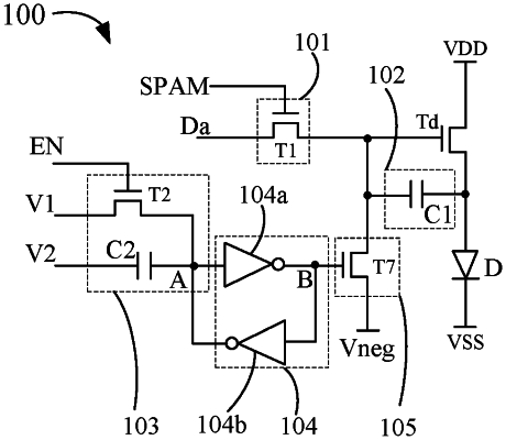
1. A light emitting circuit, comprising:
a driving transistor, wherein one of a source and a drain of the driving transistor is configured to receive a first power signal;
a light emitting device, comprising a first end electrically connected to the other of the source and the drain of the driving transistor, wherein a second end of the light emitting device is configured to receive a second power signal;
a data signal writing module, configured to receive a scan signal and a data signal and electrically connected to a gate of the driving transistor, wherein the data signal writing module is configured to write the data signal to the gate of the driving transistor under a control of the scan signal;
a first control module, configured to receive a control signal, a first voltage signal, and a second voltage signal and electrically connected to a first node, wherein the first control module is configured to control a potential of the first node under a control of the control signal, the first voltage signal, and the second voltage signal;
a bistable circuit module, configured to receive the first power signal and a third power signal and electrically connected to the first node and a second node, wherein the bistable circuit module is configured to control a potential of the second node under a control of the potential of the first node, the first power signal, and the third power signal;
a second control module, configured to receive the third power signal and electrically connected to the second node and the gate of the driving transistor, wherein the second control module is configured to control a potential of the gate of the driving transistor under a control of the potential of the second node, and the third power signal; and
a storage module, electrically connected to the gate of the driving transistor and the second end of the light emitting device, wherein the storage module is configured to maintain the potential of the gate of the driving transistor.
|