| CPC G09G 3/3266 (2013.01) [G09G 3/32 (2013.01); G09G 3/3291 (2013.01); G09G 2310/0267 (2013.01); G09G 2310/0275 (2013.01); G09G 2310/0286 (2013.01)] | 20 Claims |

|
1. A gate driver comprising
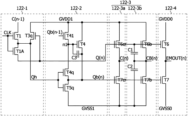
a plurality of signal transmitters connected in a cascaded manner via a carry line through which a carry signal is applied to a signal transmitter from a previous signal transmitter,
wherein an nth signal transmitter of the plurality of signal transmitter includes:
a first output circuit configured to output a carry signal to a first output node based on a voltage at a first control node and a voltage at a second control node;
a second output circuit configured to output a boosting signal to a second output node based on the voltage at the first control node and the voltage at the second control node; and
a third output circuit configured to output a gate signal to a third output node based on the voltage at the first control node and the voltage at the second control node,
wherein the second output circuit includes:
a pull-up transistor configured to apply a gate high voltage to the second output node in response to a charging voltage at the first control node;
a pull-down transistor configured to apply a gate low voltage to the second output node in response to a charging voltage at the second control node; and
a first capacitor connected between a gate of the pull-up transistor and the second output node,
wherein n is a positive integer.
|