| CPC G09G 3/3266 (2013.01) [G09G 3/32 (2013.01); G09G 2310/0267 (2013.01); G09G 2330/06 (2013.01)] | 20 Claims |

|
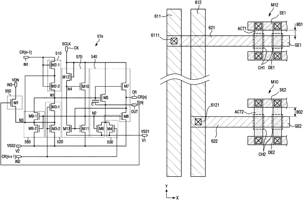
1. A scan signal driver comprising:
a plurality of stages that sequentially outputs a plurality of scan signals based on a plurality of driving voltages and a plurality of external signals received by the plurality of stages, wherein
each of the plurality of stages includes a plurality of transistors and at least one specific node electrically connected to ones of the plurality of transistors, the plurality of transistors including a plurality of first transistors and a plurality of second transistors,
each of the plurality of first transistors includes:
a first gate electrode that receives any one of the plurality of external signals;
a first semiconductor layer overlapping at least a portion of the first gate electrode, the first semiconductor layer including ‘n’ number of channel areas; and
a first source electrode and a first drain electrode spaced apart from each other by a distance, the first gate electrode disposed at a center between the first source electrode and the first drain electrode, and
each of the plurality of second transistors includes:
a second gate electrode electrically connected to any one of the at least one specific node;
a second semiconductor layer overlapping at least a portion of the second gate electrode, the second semiconductor layer including ‘m’ number of channel areas smaller than the ‘n’ number of channel areas; and
a second source electrode and a second drain electrode spaced apart from each other by a distance, the second gate electrode being disposed at a center between the second source electrode and the second drain electrode.
|