| CPC G09G 3/3266 (2013.01) [H01L 29/78648 (2013.01); H10K 59/131 (2023.02); G09G 3/3258 (2013.01); G09G 2300/0426 (2013.01); G09G 2310/0286 (2013.01); G09G 2310/0297 (2013.01); G09G 2320/0247 (2013.01); H01L 27/124 (2013.01)] | 20 Claims |

|
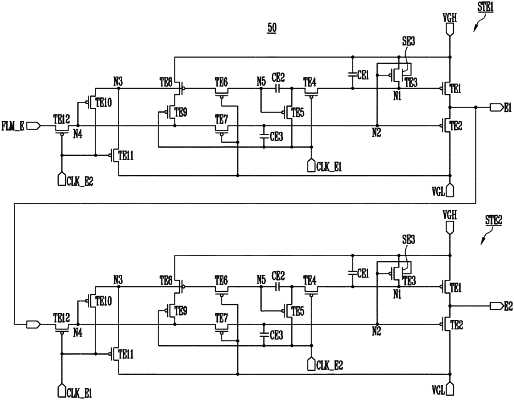
1. A display device comprising:
a first pixel coupled to an emission control line; and
an emission control stage configured to selectively couple the emission control line to a first supply voltage line or a second supply voltage line,
wherein the emission control stage comprises:
a first emission control transistor including a first electrode coupled to the first supply voltage line, a second electrode coupled to the emission control line, and a gate electrode coupled to a first node;
a second emission control transistor including a first electrode coupled to the emission control line, a second electrode coupled to the second supply voltage line, and a gate electrode coupled to a second node; and
a third emission control transistor including a first electrode coupled to the first supply voltage line, a second electrode coupled to the first node, a main gate electrode, and a sub-gate electrode, and
wherein the main gate electrode and the sub-gate electrode of the third emission control transistor are electrically coupled to the gate electrode of the second emission control transistor.
|