US 12,087,228 B2
Display apparatus having pixel including three transistors and two capacitors, and method of driving the same
Chong-Chul Chai, Seoul (KR); Oh-Kyong Kwon, Seoul (KR); Nack-Hyeon Keum, Daegu (KR); Kyong-Hwan Oh, Seoul (KR); Young-Wan Seo, Suwon-si (KR); Yong-Koo Her, Yongin-si (KR); and In-Jae Hwang, Suwon-si (KR)
Assigned to Samsung Display Co., Ltd., Yongin-si (KR); and Industry-University Cooperation Foundation Hanyang University, Seoul (KR)
Filed by Samsung Display Co., Ltd., Yongin-Si (KR); and Industry-University Cooperation Foundation Hanyang University, Seoul (KR)
Filed on Mar. 20, 2023, as Appl. No. 18/123,334.
Application 17/449,642 is a division of application No. 16/908,803, filed on Jun. 23, 2020, granted, now 11,164,525, issued on Nov. 2, 2021.
Application 16/908,803 is a division of application No. 16/391,142, filed on Apr. 22, 2019, granted, now 10,733,938, issued on Aug. 4, 2020.
Application 18/123,334 is a continuation of application No. 17/449,642, filed on Sep. 30, 2021, granted, now 11,610,547.
Application 16/391,142 is a continuation of application No. 15/400,465, filed on Jan. 6, 2017, granted, now 10,311,793, issued on Jun. 4, 2019.
Claims priority of application No. 10-2016-0061093 (KR), filed on May 18, 2016.
Prior Publication US 2023/0230546 A1, Jul. 20, 2023
This patent is subject to a terminal disclaimer.
Int. Cl. G09G 3/3258 (2016.01); G09G 3/3233 (2016.01); G09G 3/3266 (2016.01)
CPC G09G 3/3258 (2013.01) [G09G 3/3233 (2013.01); G09G 3/3266 (2013.01); G09G 2300/0426 (2013.01); G09G 2300/0819 (2013.01); G09G 2300/0852 (2013.01); G09G 2300/0866 (2013.01); G09G 2310/063 (2013.01); G09G 2320/02 (2013.01); G09G 2320/043 (2013.01); G09G 2330/021 (2013.01)] 8 Claims
OG exemplary drawing
 
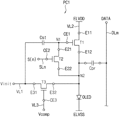
1. A display panel comprising:
a plurality of pixels, wherein a pixel of the plurality of pixels comprises:
a light emitting element;
a first transistor comprising a control electrode connected to a first node, a first electrode configured to receive a first power source signal and a second electrode connected to a first electrode of the light emitting element;
a first capacitor connected between an initialization electrode and the first node;
a second transistor comprising a control electrode configured to receive a scan signal, a first electrode connected to the first node and a second electrode connected to a first electrode of a second capacitor; and
the second capacitor comprising the first electrode directly connected to the second electrode of the second transistor and a second electrode configured to receive a data voltage from a data line,
wherein no transistor is connected between the second electrode of the second transistor and the data line.