| CPC G09G 3/32 (2013.01) [G09G 2300/0443 (2013.01); G09G 2310/0267 (2013.01); G09G 2310/0275 (2013.01); G09G 2320/0233 (2013.01)] | 29 Claims |

|
1. A display panel, comprising:
a substrate;
a plurality of pixels on the substrate each including sub pixels; and
a gate driver formed directly on the substrate together with the pixels,
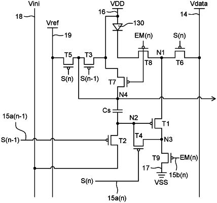
wherein the pixel includes a light emitting diode including an anode electrode and a cathode electrode, the anode electrode being electrically connected to a first power line to which a high potential voltage is supplied,
wherein each of the sub pixels includes:
a driving element in which a source is connected to a N1 node, a gate is connected to a N2 node, and a drain is connected to a N3 node,
a capacitor connected to the N2 node and a N4 node;
a N1 switching circuit connected to the N1 node;
a N2 switching circuit connected to the N2 node;
a N3 switching circuit connected to the N3 node; and
a N4 switching circuit connected to the N4 node, and
wherein the light emitting diode is electrically connected between the first power line and the driving element, and
wherein the N4 switching circuit is connected to a fourth power line which supplies a reference voltage, and a driving current value generated by the driving element while the light emitting diode emits light is determined based on the reference voltage.
|