| CPC G06V 40/1318 (2022.01) [G09G 3/3233 (2013.01); H10K 39/34 (2023.02); H10K 59/1213 (2023.02); H10K 59/40 (2023.02); G09G 2300/0426 (2013.01); G09G 2300/0819 (2013.01); G09G 2300/0842 (2013.01); G09G 2300/0861 (2013.01); G09G 2310/08 (2013.01); G09G 2354/00 (2013.01)] | 27 Claims |

|
1. A display device comprising:
a base layer; and
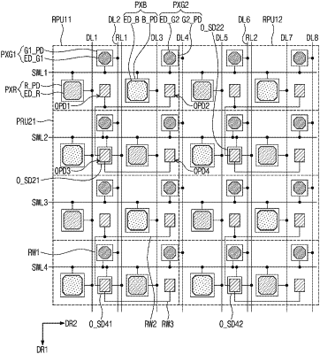
a pixel layer disposed on the base layer, the pixel layer including a plurality of pixels and a plurality of sensors,
wherein each of the plurality of pixels includes:
a light emitting element, and
a pixel drive circuit connected to the light emitting element to control driving of the light emitting element, and
wherein each of the plurality of sensors includes:
a light sensing unit including a plurality of light sensing elements,
a sensor drive circuit connected to at least two light sensing elements and configured to output a sensing signal in response to light, and
a routing wire configured to electrically connect the at least two light sensing elements to each other.
|