| CPC G06V 40/1318 (2022.01) [G06F 1/1656 (2013.01); G06F 3/0412 (2013.01); G06F 3/0421 (2013.01); G06F 2203/04103 (2013.01)] | 17 Claims |

|
1. An electronic device comprising:
a display;
a support member having a first hole and configured to support the display;
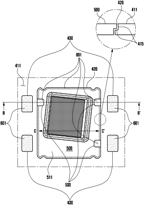
a first fingerprint sensor disposed in the first hole such that there is a space between the first fingerprint sensor and the support member forming a perimeter around the first fingerprint sensor, wherein the first fingerprint sensor has a top surface facing the display, and a bottom surface opposite to the top surface;
a non-conductive injection molding material bonding the first fingerprint sensor to the support member, wherein the non-conductive injection molding material fills the space between the first fingerprint sensor and the support member and covering the bottom surface of the first fingerprint sensor; and
a printed circuit board disposed on one surface of the support member, wherein the first fingerprint sensor is connected to the printed circuit board through a signal connection member, and a portion of the signal connection member is embedded in the non-conductive injection molding material,
wherein the first fingerprint sensor comprises a plurality of sensing pixels and an elastic member, and
wherein the elastic member is disposed under the display such that an air gap is formed between the display and the plurality of sensing pixels.
|