| CPC G06V 40/1318 (2022.01) [G06V 40/1306 (2022.01); H01L 25/167 (2013.01); H01L 27/14636 (2013.01); H01L 27/14643 (2013.01)] | 16 Claims |

|
1. A display panel, comprising:
a thin-film transistor (TFT) device layer, wherein the TFT device layer comprises a source, a drain, a gate, and an active layer of a TFT;
a planarization layer, wherein the planarization layer is disposed on the TFT device layer;
a first electrode layer, wherein the first electrode layer is disposed on the planarization layer; and
a storage capacitor, wherein the storage capacitor is disposed on a side of the TFT device layer;
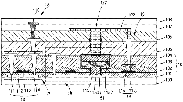
wherein the display panel further comprises a fingerprint recognition module, the fingerprint recognition module comprises a sensing electrode layer, the sensing electrode layer and the active layer are disposed on a same layer, the storage capacitor is electrically connected to the fingerprint recognition module by the first electrode layer, a material of the first electrode layer is indium tin oxide (ITO), and the fingerprint recognition module comprises at least one of a light fingerprint recognition device or an ultrasonic fingerprint recognition device, wherein the fingerprint recognition module further comprises a photosensitive electrode layer, an end of the photosensitive electrode layer is connected to the first electrode layer, and another end of the photosensitive electrode layer is connected to the sensing electrode layer; wherein the photosensitive electrode layer comprises a first photosensitive electrode, a second photosensitive electrode, and a connecting layer, the first photosensitive electrode is disposed on the connecting layer, and the second photosensitive electrode is disposed on the first photosensitive electrode, the first photosensitive electrode is electrically connected to the sensing electrode layer by the connecting layer, and the second photosensitive electrode is electrically connected to the first electrode layer;
wherein a width of the connecting layer is less than a width of the first photosensitive electrode, and the width of the first photosensitive electrode is less than or equal to a width of the second photosensitive electrode.
|