| CPC G06F 9/44573 (2013.01) [G06F 3/0604 (2013.01); G06F 3/0659 (2013.01); G06F 3/0679 (2013.01); G06F 9/4403 (2013.01); G06F 11/1068 (2013.01); G06F 12/0868 (2013.01); G06F 13/1668 (2013.01); G06F 13/4282 (2013.01); G11C 16/0483 (2013.01); G11C 16/26 (2013.01); G11C 16/32 (2013.01); G06F 2212/60 (2013.01)] | 15 Claims |

|
1. A device comprising:
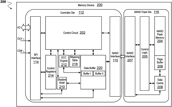
a NAND flash memory configured to store data;
a non-volatile register configured to record source addresses for data transition;
a shadow RAM connected with the NAND flash memory through a data cache from the NAND flash memory to the shadow RAM; and
a control circuit connected with the NAND flash memory and the shadow RAM, wherein the control circuit is configured to:
determine, based on power on of an electronic device, a location of first data in a NAND flash memory of the electronic device, and
transmit the first data to a shadow RAM of the electronic device.
|