| CPC G06F 3/0445 (2019.05) | 18 Claims |

|
1. A touch display device comprising:
a plurality of light-emitting elements on an active area of a display panel;
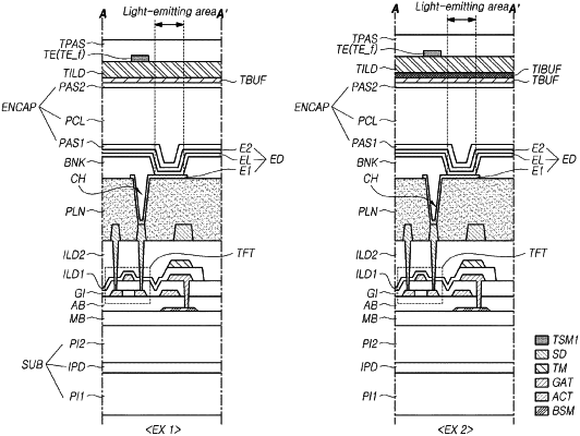
an encapsulation layer on the plurality of light-emitting elements;
a first touch sensor metal on the encapsulation layer and comprising a plurality of touch electrodes and a plurality of touch routing lines electrically connected to the plurality of touch electrodes, the plurality of touch routing lines extending to a pad area positioned outside of the encapsulation layer;
a planarization layer on the encapsulation layer, the planarization layer extending to an area between the active area and the pad area;
a first touch insulating layer on the planarization layer;
a second touch sensor metal on the first touch insulating layer and comprising a plurality of touch electrode connecting patterns and a plurality of auxiliary routing patterns; and
a second touch insulating layer on the first touch insulating layer;
wherein the first touch insulating layer includes an inorganic material and the second touch insulating layer includes an organic material, and
wherein the second touch insulating layer covers the plurality of auxiliary routing patterns.
|