| CPC G06F 3/04164 (2019.05) [H05K 1/142 (2013.01); G06F 3/0446 (2019.05); G06F 2203/04111 (2013.01); H05K 1/18 (2013.01); H05K 1/189 (2013.01); H05K 2201/049 (2013.01); H10K 59/40 (2023.02)] | 17 Claims |

|
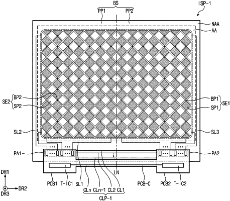
1. A display device comprising:
a base layer including an active area and a non-active area adjacent to the active area;
a first circuit board and a second circuit board disposed on the non-active area and spaced apart from each other;
a first circuit chip mounted on the first circuit board and a second circuit chip mounted on the second circuit board,
wherein the base layer is of a rectangular shape with a short side extending in a first direction and a long side extending in a second direction different from the first direction,
wherein the base layer is divided into a first part and a second part by a first imaginary line dividing the long side,
wherein the first circuit board overlaps the non-active area and is disposed on the first part,
wherein the second circuit board overlaps the non-active area and is disposed on the second part, and
wherein no intervening circuit chip is disposed between the first circuit chip and the second circuit chip;
more than two connection lines directly connecting the first circuit chip and the second circuit chip with each other,
wherein the more than two connection lines comprise a power line, a communication line, and a ground line, and
wherein the ground line, among the more than two connection lines, extends lengthwise along the long side of the base layer and is the most distant from the active area; and
a connection circuit board partially overlapping the non-active area of the base layer in a vertical direction and physically connecting the first circuit board to the second circuit board,
wherein the connection circuit board is integrated with the first and second circuit boards, and
wherein at least two of the more than two connection lines are disposed on the connection circuit board.
|