| CPC G06F 3/041 (2013.01) [G06F 2203/04112 (2013.01)] | 20 Claims |

|
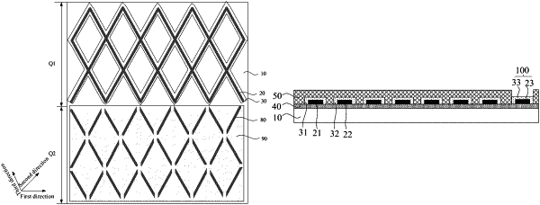
1. A thin film sensor, comprising:
a base substrate;
a first conductive mesh on the base substrate; wherein the first conductive mesh comprises a plurality of first metal wires arranged side by side along a first direction and each extending in a second direction, and a plurality of second metal wires arranged side by side along the first direction and each extending in a third direction; and the plurality of first metal wires intersect with the plurality of second metal wires; and
a second conductive mesh on a side of the first conductive mesh away from the base substrate;
wherein the second conductive mesh comprises a plurality of first transparent conductive wires arranged side by side along the first direction and each extending in the second direction, and a plurality of second transparent conductive wires arranged side by side along the first direction and each extending in the third direction; and the plurality of first transparent conductive wires intersect with the plurality of second transparent conductive wires; and wherein each of the plurality of first transparent conductive wires has an orthographic projection on the base substrate covering an orthographic projection of one of the plurality of first metal wires on the base substrate; and each of the plurality of second transparent conductive wires has an orthographic projection on the base substrate covering an orthographic projection of one of the plurality of second metal wires on the base substrate.
|