US 12,086,088 B2
Multichip package with protocol-configurable data paths
Huy Ngo, San Jose, CA (US); Keith Duwel, San Jose, CA (US); and David W. Mendel, Sunnyvale, CA (US)
Assigned to Altera Corporation, San Jose, CA (US)
Filed by Altera Corporation, San Jose, CA (US)
Filed on Apr. 24, 2023, as Appl. No. 18/306,100.
Application 18/306,100 is a continuation of application No. 17/711,860, filed on Apr. 1, 2022, granted, now 11,669,479.
Application 17/711,860 is a continuation of application No. 17/131,474, filed on Dec. 22, 2020, granted, now 11,294,842, issued on Apr. 5, 2022.
Application 17/131,474 is a continuation of application No. 16/436,771, filed on Jun. 10, 2019, granted, now 10,884,964, issued on Jan. 5, 2021.
Application 16/436,771 is a continuation of application No. 14/975,270, filed on Dec. 18, 2015, granted, now 10,394,737, issued on Aug. 27, 2019.
Prior Publication US 2023/0289309 A1, Sep. 14, 2023
This patent is subject to a terminal disclaimer.
Int. Cl. G06F 13/40 (2006.01); G06F 5/06 (2006.01); G06F 13/42 (2006.01)
CPC G06F 13/4022 (2013.01) [G06F 5/065 (2013.01); G06F 13/4018 (2013.01); G06F 13/4291 (2013.01); G06F 2205/067 (2013.01)] 20 Claims
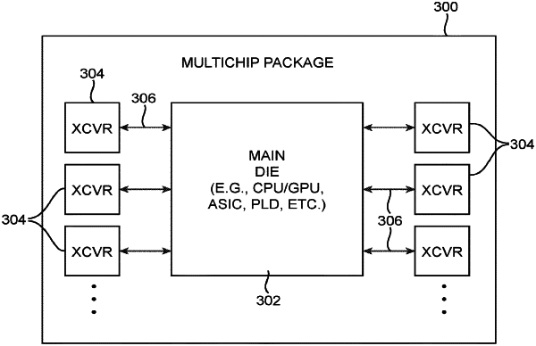
OG exemplary drawing
 
1. A system comprising:
a first die of a first single package multi-die device having first input/output circuitry; and
a second die of the first single package multi-die device communicatively coupled to the first die, wherein the second die comprises second input/output circuitry configurable to operate in:
a first mode in which a read clock frequency or a write clock frequency is a first frequency; and
a second mode in which the read clock frequency or the write clock frequency is a second frequency that is different than the first frequency.