| CPC G06F 12/1045 (2013.01) [G06F 7/24 (2013.01); G06F 7/487 (2013.01); G06F 7/4876 (2013.01); G06F 7/49915 (2013.01); G06F 7/53 (2013.01); G06F 7/57 (2013.01); G06F 9/3001 (2013.01); G06F 9/30014 (2013.01); G06F 9/30021 (2013.01); G06F 9/30032 (2013.01); G06F 9/30036 (2013.01); G06F 9/30065 (2013.01); G06F 9/30072 (2013.01); G06F 9/30098 (2013.01); G06F 9/30112 (2013.01); G06F 9/30145 (2013.01); G06F 9/30149 (2013.01); G06F 9/3016 (2013.01); G06F 9/32 (2013.01); G06F 9/345 (2013.01); G06F 9/3802 (2013.01); G06F 9/3818 (2013.01); G06F 9/383 (2013.01); G06F 9/3836 (2013.01); G06F 9/3851 (2013.01); G06F 9/3856 (2023.08); G06F 9/3867 (2013.01); G06F 9/3887 (2013.01); G06F 9/48 (2013.01); G06F 11/00 (2013.01); G06F 11/1048 (2013.01); G06F 12/0862 (2013.01); G06F 12/0875 (2013.01); G06F 12/0897 (2013.01); G06F 12/1009 (2013.01); G06F 17/16 (2013.01); H03H 17/0664 (2013.01); G06F 9/30018 (2013.01); G06F 9/325 (2013.01); G06F 9/381 (2013.01); G06F 9/3822 (2013.01); G06F 11/10 (2013.01); G06F 15/7807 (2013.01); G06F 15/781 (2013.01); G06F 2212/452 (2013.01); G06F 2212/60 (2013.01); G06F 2212/602 (2013.01); G06F 2212/68 (2013.01)] | 20 Claims |

|
1. A device comprising:
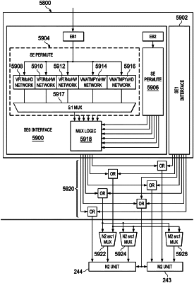
a cache controller interface configured to receive a set of data elements, wherein the cache controller interface includes:
a buffer configured to store the set of data elements;
a first circuit coupled to the buffer and configured to reorder bits of the set of data elements according to a first finite impulse response operation to produce the set of data elements in a first arrangement;
a second circuit coupled to the buffer in parallel with the first circuit and configured to reorder the bits of the set of data elements according to a second finite impulse response operation to produce the set of data elements in a second arrangement that is different from the first arrangement; and
a selection circuit coupled to the first circuit and the second circuit and configured to select between providing the set of data elements in the first arrangement or the set of data elements in the second arrangement; and
a processor functional unit coupled to the selection circuit and configured to selectably perform either the first finite impulse response operation or the second finite impulse response operation on the set of data elements.
|