| CPC G06F 12/0811 (2013.01) [G06F 12/10 (2013.01); G06F 2212/608 (2013.01)] | 20 Claims |

|
1. An apparatus comprising:
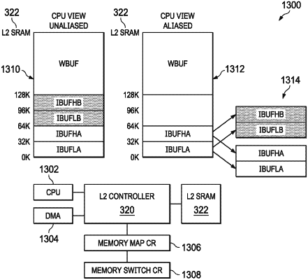
a memory including a first portion and a second portion;
a memory switch control register;
a memory map control register; and
a memory controller coupled to the memory, the memory map control register, and the memory switch control register, wherein the memory controller is configured to:
receive a first memory access instruction associated with a virtual address associated with the first portion;
receive a second memory access instruction associated with the virtual address; and
in response to the memory map control register indicating an aliased mode and the memory switch control register indicating a first value:
direct the first memory access instruction to a first physical address in the first portion of the memory; and
direct the second memory access instruction to a second physical address in the second portion of the memory.
|