| CPC G06F 1/1652 (2013.01) [G06F 1/181 (2013.01); G06F 1/189 (2013.01); G09F 9/301 (2013.01); H01L 33/48 (2013.01)] | 19 Claims |

|
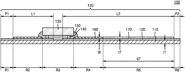
1. A chip-on-film (COF) package comprising:
a film including a reinforcement area, a bending area, and a chip mounting area, wherein the reinforcement area is between the chip mounting area and the bending area;
a conductive pattern layer disposed on the film in the reinforcement area, in the bending area, and at in the chip mounting area;
a chip mounted on a portion of the conductive pattern layer in the chip mounting area;
a first insulating layer having a first elastic modulus and extending over the conductive pattern layer in the reinforcement area, wherein a portion of the first insulating layer closest to the bending area terminates outside the bending area; and
a second insulating layer having a second elastic modulus and extending over the conductive pattern layer in the bending area and reinforcement area,
wherein the first elastic modulus is greater than the second elastic modulus, and the first elastic modulus is in a range of from about 5 GPa to about 20 GPa, and the second elastic modulus is in a range of from about 0.5 GPa to about 2 GPa, and
wherein the second insulating layer is positioned between the conductive pattern layer and the first insulating layer.
|