| CPC G06F 1/1637 (2013.01) [G02F 1/0063 (2013.01); G06F 1/1658 (2013.01); G06F 3/0412 (2013.01); H04M 1/0264 (2013.01); H04M 1/0266 (2013.01); G06F 2200/16 (2013.01); G06F 2203/041 (2013.01)] | 20 Claims |

|
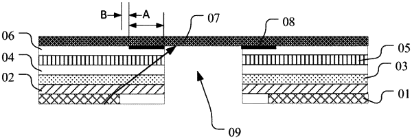
1. A display panel, wherein the display panel comprises:
an array substrate, comprising a base substrate and a light-emitting layer;
a composite functional layer, located on a side of the light-emitting layer away from the base substrate, wherein a through hole penetrating the composite functional layer and the array substrate is formed in the array substrate and the composite functional layer;
wherein, the array substrate comprises a non-display area surrounding the through hole, the composite functional layer comprises a first shading layer, and an orthographic projection of the first shading layer on the array substrate is located in the non-display area of the array substrate;
a first adhesive layer, located on a side of the composite functional layer away from the base substrate; and
a cover plate, located on a side of the first adhesive layer away from the base substrate,
wherein the light-emitting layer comprises a plurality of light-emitting units, and the composite functional layer further comprises:
a color film layer, comprising a plurality of color filter parts and a shading part located among the plurality of the color filter parts, wherein the plurality of the color filter parts and the plurality of the light-emitting units are arranged in one-to-one correspondence, and an orthographic projection of a color filter part on the base substrate at least partially overlaps with an orthographic projection of a corresponding light-emitting unit on the base substrate; and
wherein, the shading part and the first shading layer are formed on a same structural layer of the array substrate, the shading part and the first shading layer are formed of a same material, and an orthographic projection of the color film layer on the base substrate surrounds at least part of an orthographic projection of the first shading layer on the array substrate.
|