| CPC G06F 1/06 (2013.01) [H03L 7/08 (2013.01)] | 13 Claims |

|
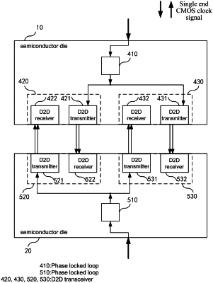
1. A semiconductor die, comprising:
a first die to die (D2D) transceiver, comprising:
a first D2D transmitter, configured to send data to a second D2D receiver in a second D2D transceiver of another semiconductor die using a first reference clock signal; and
a first D2D receiver, configured to receive data from a second D2D transmitter in the second D2D transceiver using a second reference clock signal,
a P2P link, configured to establish a communication channel with an external electronic device to transmit the data, the P2P link comprising:
a first P2P sub-link, configured to establish a first communication channel with the external electronic device to transmit the data using a fourth reference clock signal from outside the semiconductor die or a second phase locked loop.
|