| CPC G05F 1/56 (2013.01) [H03K 5/08 (2013.01); H03K 17/6872 (2013.01)] | 20 Claims |

|
1. A voltage driver for supplying a supply voltage (vddio), comprising:
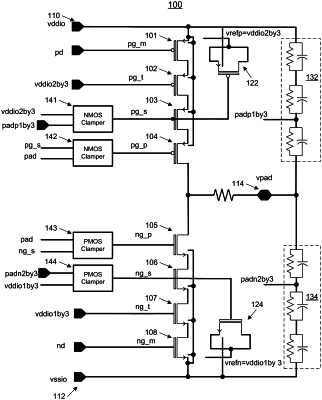
a plurality of PMOS transistors connected in series and a plurality of NMOS transistors connected in series, each PMOS transistor of the plurality of PMOS transistors or NMOS transistor of the plurality of NMOS transistors having a drain-source voltage between a drain terminal and a source terminal (vdd), and a maximum of the supply voltage is N times a maximum of the drain-source voltage, where N>2;
a pad configured to receive a voltage signal (vpad) for controlling gates of a subset of the plurality of NMOS transistors and a subset of the plurality of PMOS transistors;
a first impedance divider circuit between the supplied voltage and the pad configured to generate a first limited voltage signal that is a fraction of a voltage (padp) between the pad and vddio;
a second impedance divider circuit between the pad and ground configured to generate a second limited voltage signal that is a fraction of a voltage (padn) between the pad and ground;
a plurality of NMOS clampers, comprising:
a first NMOS clamper configured to receive the first limited voltage signal and a first reference voltage (vrefp) as input, and output a first NMOS clamper output signal to a gate of a first PMOS transistor among the subset of PMOS transistors, and
a second NMOS clamper configured to receive at least the first NMOS clamper output signal as input, and output a second NMOS clamper output signal to a gate of a second PMOS transistor among the subset of PMOS transistors, the first or second NMOS clamper comprising a pair of NMOS transistors; and
a plurality of PMOS clampers, comprising:
a first PMOS clamper configured to receive the second limited voltage signal and a second reference voltage (vrefn) as input, and output first PMOS clamper output signal to a gate of a first NMOS transistor among the subset of NMOS transistors, and
a second PMOS clamper configured to receive at least the first PMOS clamper output signal as input, and output a second PMOS clamper output signal to a gate of a second NMOS transistor among the subset of NMOS transistors, the first or second PMOS clamper comprising a pair of PMOS transistors.
|