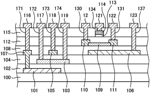
| CPC G02F 1/136286 (2013.01) [G02F 1/136227 (2013.01); G02F 1/1368 (2013.01); H01L 27/124 (2013.01); H01L 29/78672 (2013.01); H10K 59/131 (2023.02); G02F 2201/123 (2013.01)] | 5 Claims |

|
1. A semiconductor device including a substrate having a first TFT (thin film transistor) and a second TFT, wherein
the first TFT has a first semiconductor layer comprising oxide semiconductor, a first gate insulating film, a first gate electrode, a first drain electrode and a first source electrode,
a passivation film is formed covering the first gate electrode,
the second TFT has a second semiconductor layer, a second gate insulating film, a second gate electrode, a second drain electrode and a second source electrode,
an interlayer insulating film is arranged between the first semiconductor layer and the second semiconductor layer,
the first semiconductor layer is disposed in an upper layer than the second semiconductor layer,
the first drain electrode is connected to the first semiconductor layer via a first through hole formed in the first gate insulating film,
the first source electrode is connected to the first semiconductor layer via a second through hole formed in the first gate insulating film,
a gate wiring is extended in a first direction, a signal wiring is extended in a second direction crossing the first direction,
the first semiconductor layer has a bent portion and is arranged to intersect the gate wiring, in a plan view,
the signal wiring is formed on the passivation film,
the signal wiring connects to the first drain electrode via a third through hole formed in the passivation film, and
a light shading film is arranged below the first semiconductor layer and overlaps the first semiconductor layer in plan view.
|