| CPC G02F 1/133512 (2013.01) [G02F 1/1339 (2013.01); G02F 1/13439 (2013.01); G02F 1/1345 (2013.01); G02F 1/13454 (2013.01); G02F 1/136209 (2013.01)] | 7 Claims |

|
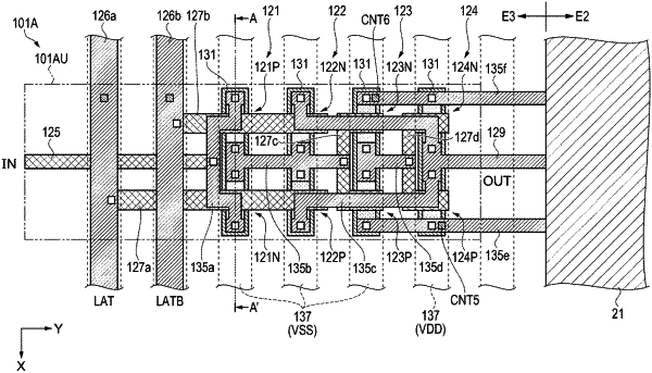
1. An electro-optical device comprising:
a photo-curable type seal material;
a first transistor disposed at a position that overlaps the photo-curable type seal material;
a second transistor disposed at a position that overlaps the photo-curable type seal material;
a third transistor disposed at a position that overlaps the photo-curable type seal material;
a fourth transistor disposed at a position that overlaps the photo-curable type seal material;
a fifth transistor disposed at a position that overlaps the photo-curable type seal material;
a sixth transistor disposed at a position that overlaps the photo-curable type seal material;
a first wiring layer disposed between the first transistor and the photo-curable type seal material in a thickness direction of the photo-curable type seal material and is disposed between the second transistor and the photo-curable type seal material in the thickness direction;
a second wiring layer disposed between the third transistor and the photo-curable type seal material in the thickness direction and is disposed between the fourth transistor and the photo-curable type seal material in the thickness direction; and
a third wiring layer disposed between the fifth transistor and the photo-curable type seal material in the thickness direction and is disposed between the sixth transistor and the photo-curable type seal material in the thickness direction, wherein
the first transistor and the second transistor are arranged along a first direction,
the first transistor, the third transistor and the fifth transistor are arranged along a second direction that intersects the first direction in plan view,
the third transistor and the fourth transistor are arranged along the first direction,
the second transistor, the fourth transistor and the sixth transistor are arranged along the second direction,
the fifth transistor and the sixth transistor are arranged along the first direction,
the first wiring layer is extend along the first direction in plan view,
the second wiring layer is extend along the second direction in plan view, and
the third wiring layer is extend along the second direction in plan view.
|