| CPC G02B 6/34 (2013.01) [G02B 6/305 (2013.01)] | 20 Claims |

|
1. A method for forming an optical coupler, comprising:
forming an insulation layer on a semiconductor substrate;
epitaxially growing a semiconductor material on the insulation layer to form a semiconductor layer;
etching, according to a predetermined pattern, the semiconductor layer to form:
an array of etched holes in the semiconductor layer to form a grating region,
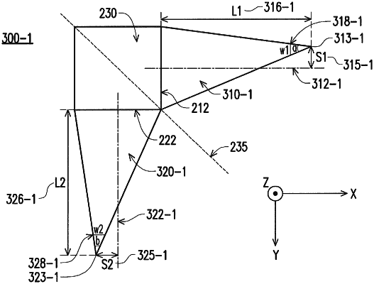
a first taper structure extending from a first side of the grating region, wherein a shape of the first taper structure in the semiconductor layer is a first triangle that is asymmetric about any line perpendicular to the first side of the grating region, and
a second taper structure extending from a second side of the grating region,
wherein a shape of the second taper structure in the semiconductor layer is a second triangle that is asymmetric about any line perpendicular to the second side of the grating region, wherein the first side and the second side are substantially perpendicular to each other; and
depositing a dielectric material into the array of etched regions to form an array of scattering elements in the semiconductor layer, wherein the scattering elements are arranged to form a two-dimensional (2D) grating.
|