| CPC G02B 27/0172 (2013.01) [G02B 6/12004 (2013.01); G02B 6/12007 (2013.01); G02B 6/125 (2013.01); G02B 27/0093 (2013.01); H10N 50/10 (2023.02); G02B 2006/12104 (2013.01); G02B 2027/0178 (2013.01)] | 20 Claims |

|
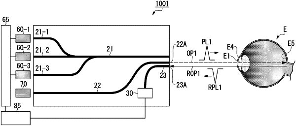
1. An optical waveguide detection element comprising:
a substrate;
an optical waveguide layer formed on the substrate; and
a photodetector,
wherein the optical waveguide layer includes:
a first optical waveguide in which visible light having a wavelength of 380 nm to 800 nm propagates;
a second optical waveguide in which near-infrared light having a wavelength of 801 nm to 2000 nm propagates; and
a third optical waveguide in which light propagates to a light receiving surface of the photodetector, and
wherein a visible light output port of the first optical waveguide from which the visible light is output, a near-infrared light output port of the second optical waveguide from which the near-infrared light is output, and a reflected light input port of the third optical waveguide to which the near-infrared light is reflected and returned are arranged on one end surface of the optical waveguide layer.
|