| CPC G01S 7/4811 (2013.01) [H01L 31/02005 (2013.01); H01L 31/02164 (2013.01); H01L 31/02327 (2013.01)] | 18 Claims |

|
1. A light-receiving element, comprising:
an on-chip lens;
a wiring layer; and
a semiconductor layer between the on-chip lens and the wiring layer, wherein
the semiconductor layer includes:
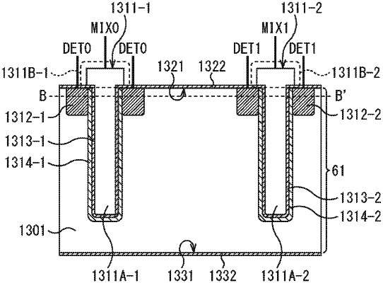
a first voltage application portion configured to receive a first voltage,
a second voltage application portion configured to receive a second voltage different from the first voltage,
a first charge detection portion around the first voltage application portion, and
a second charge detection portion around the second voltage application portion,
an insulating film that covers each of the first voltage application portion and the second voltage application portion, and
a hole concentration strengthening layer on an outer periphery of the insulating film.
|