| CPC G01N 21/9501 (2013.01) [G01N 21/3563 (2013.01); G01N 21/59 (2013.01); G01N 2021/3568 (2013.01); G01N 2021/3595 (2013.01)] | 20 Claims |

|
1. A system for non-contact characterization of a semiconductor device under test comprising:
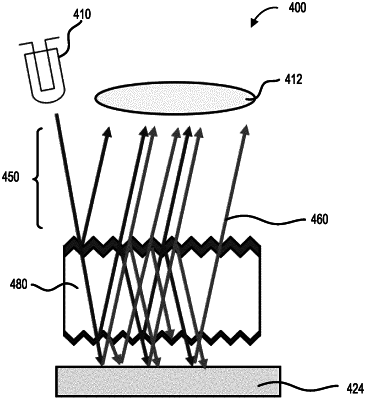
an infrared radiation source directing radiation towards the semiconductor device;
a radiation directing device positioned proximal the infrared radiation source and configured to direct radiation towards an opposing side of the semiconductor device, the semiconductor device receivable between the radiation directing device and the infrared radiation source; and
a radiation detector proximal to the infrared radiation source and configured to sense radiation associated with a plurality of infrared wavebands from the semiconductor device for determining a dopant profile property of the semiconductor device, the sensed radiation including radiation originating from the infrared radiation source reflected from the semiconductor device, the sensed radiation including radiation originating from the radiation directing device and emerging from the semiconductor device,
wherein the dopant profile properties based on at least one of infrared reflectance or infrared transmittance associated with the plurality of respective infrared wavebands.
|