| CPC G01B 11/27 (2013.01) [G01B 11/0608 (2013.01); G03F 7/70633 (2013.01); G03F 7/7085 (2013.01); G03F 9/7088 (2013.01); H01L 21/67259 (2013.01)] | 8 Claims |

|
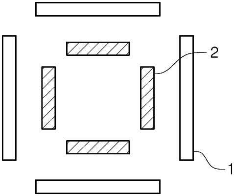
1. An overlay measurement device for measuring an error between a first overlay mark and a second overlay mark respectively formed on different layers formed on a wafer, comprising:
a first light source configured to irradiate a first beam;
a first detector configured to acquire a signal by the first beam emitted from the first light source and reflected at a measurement position of the wafer;
a second light source configured to irradiate a second beam having a wavelength different from the wavelength of the first beam;
a second detector configured to acquire a signal by the second beam emitted from the second light source and reflected at the measurement position of the wafer;
an objective lens configured to condense the first beam and the second beam at the measurement position of the wafer and collect the beam reflected at the measurement position;
an actuator configured to adjust a relative position of the objective lens with respect to the wafer in an optical axis direction;
a controller configured to control the actuator; and
a detector configured to detect a height of the first overlay mark based on a change in the signal of the first detector according to a change in the relative position of the objective lens with respect to the wafer in the optical axis direction and detect a height of the second overlay mark based on a change in the signal of the second detector according to a change in the relative position of the objective lens with respect to the wafer in the optical axis direction.
|